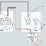
A Sch11 Wiring Diagram is a circuit layout that shows the connections between the various components within a Sch11 microchip. It provides a detailed representation of the chip’s internal architecture, allowing engineers to analyze and troubleshoot issues, as well as make modifications or enhancements.
These diagrams are essential for understanding the functionality and capabilities of a Sch11 microchip. They enable designers to develop and debug circuits, optimize performance, and ensure reliability. By providing a visual representation of the chip’s internal workings, Sch11 Wiring Diagrams facilitate efficient hardware design and troubleshooting processes.
Historically, Sch11 Wiring Diagrams were manually drawn using specialized software or tools. Today, advanced computer-aided design (CAD) software automates the creation of these diagrams, significantly reducing design time and improving accuracy. This advancement has made Sch11 microchips more accessible and widely used in various electronic systems.
Understanding the essential aspects of Sch11 Wiring Diagrams is crucial for effectively utilizing these diagrams in electronic system design. These aspects encompass various dimensions related to the diagram’s structure, function, and significance.
- Circuit Layout: Sch11 Wiring Diagrams depict the physical arrangement and interconnections of components within the microchip.
- Signal Flow: These diagrams illustrate the paths taken by electrical signals as they traverse the microchip, providing insights into the chip’s functionality.
- Component Interfacing: The diagram shows how different components within the microchip interact and communicate with each other.
- Power Distribution: Sch11 Wiring Diagrams indicate the power supply connections and distribution throughout the microchip, ensuring stable and reliable operation.
- Grounding: Proper grounding is essential for reducing noise and ensuring signal integrity. Wiring diagrams provide a visual representation of the grounding scheme implemented within the microchip.
- Testing and Debugging: These diagrams serve as valuable tools for testing, troubleshooting, and debugging circuits, facilitating the detection and resolution of issues.
- Documentation: Sch11 Wiring Diagrams provide comprehensive documentation of the microchip’s internal design, aiding in maintenance, repair, and future modifications.
- Industry Standards: Wiring diagrams adhere to established industry standards, ensuring compatibility and interoperability with other electronic components and systems.
These essential aspects collectively contribute to the effective design, analysis, and maintenance of electronic circuits incorporating Sch11 microchips. Understanding these aspects enables engineers to harness the full potential of these diagrams and optimize system performance.
Circuit Layout
In the context of Sch11 Wiring Diagrams, circuit layout holds paramount importance. These diagrams provide a detailed visual representation of the physical arrangement and interconnections of various components within the Sch11 microchip. Understanding this circuit layout is essential for analyzing, troubleshooting, and modifying the chip’s functionality.
- Component Placement: Sch11 Wiring Diagrams show the specific locations and orientations of transistors, resistors, capacitors, and other components on the microchip. This information is crucial for understanding the signal flow and interactions between components.
- Signal Routing: The diagrams depict the paths taken by electrical signals as they traverse the microchip. This includes tracing the connections between input/output pins and internal components, providing insights into the chip’s functionality and performance.
- Power Distribution: Sch11 Wiring Diagrams indicate the power supply connections and distribution throughout the microchip. This information is critical for ensuring stable and reliable operation, as well as for troubleshooting power-related issues.
- Grounding Scheme: Wiring diagrams also show the grounding scheme implemented within the microchip. Proper grounding is essential for reducing noise and ensuring signal integrity, making this aspect crucial for understanding the chip’s stability and performance.
By providing a comprehensive overview of the circuit layout, Sch11 Wiring Diagrams empower engineers to effectively design, analyze, and maintain electronic circuits incorporating Sch11 microchips. These diagrams serve as invaluable tools for optimizing system performance, troubleshooting issues, and ensuring reliability.
Signal Flow
Signal flow plays a pivotal role in understanding the operation of an Sch11 microchip. Sch11 Wiring Diagrams provide detailed insights into the paths taken by electrical signals as they traverse the microchip’s internal circuitry, enabling engineers to analyze and optimize its functionality. By examining the signal flow, one can gain a comprehensive understanding of how the chip processes and transmits data, making it easier to troubleshoot issues and implement design modifications.
- Signal Routing: Sch11 Wiring Diagrams depict the specific paths taken by electrical signals as they flow through the microchip. This information is crucial for understanding the chip’s functionality and performance, as it reveals the connections between input/output pins and internal components.
- Signal Timing: These diagrams also provide insights into the timing characteristics of the signals, including propagation delays and clock synchronization. This information is essential for ensuring that the microchip operates reliably and efficiently within the desired timing constraints.
- Signal Integrity: Sch11 Wiring Diagrams help identify potential sources of signal noise and interference. By understanding the signal flow, engineers can implement appropriate measures to mitigate these issues and ensure the integrity of the transmitted signals.
- Signal Conditioning: Wiring diagrams also reveal the presence of signal conditioning circuits, such as amplifiers, filters, and level shifters. These circuits play a crucial role in shaping and adapting signals to meet the specific requirements of different components within the microchip.
In summary, understanding the signal flow in Sch11 microchips is critical for effective circuit design, analysis, and troubleshooting. Sch11 Wiring Diagrams provide invaluable insights into the signal paths, timing characteristics, and signal integrity aspects of the microchip, empowering engineers to optimize system performance and ensure reliable operation.
Component Interfacing
In the context of Sch11 Wiring Diagrams, understanding component interfacing is essential for analyzing and optimizing the functionality of Sch11 microchips. These diagrams provide detailed insights into how different components within the microchip interact and communicate, enabling engineers to identify potential issues, implement design modifications, and ensure reliable operation.
- Data Transfer: Sch11 Wiring Diagrams reveal the data transfer mechanisms between different components, including buses, registers, and memory units. This information is crucial for understanding how data is exchanged and processed within the microchip.
- Control Signals: These diagrams also show the flow of control signals, such as clock signals, reset signals, and interrupt signals. Understanding these signals is essential for ensuring proper synchronization and communication between components.
- Input/Output Interfacing: Sch11 Wiring Diagrams depict the connections between the microchip’s input/output pins and internal components. This information is vital for interfacing the microchip with external devices and peripherals.
- Power Management: Wiring diagrams also provide insights into the power management scheme of the microchip, including power supply connections, voltage regulators, and power distribution networks. This information is crucial for ensuring stable and reliable operation of the microchip.
In summary, component interfacing plays a critical role in the design and analysis of Sch11 microchips. Sch11 Wiring Diagrams provide comprehensive insights into the interactions and communication between different components within the microchip, empowering engineers to optimize system performance, troubleshoot issues, and ensure reliable operation.
Power Distribution
Understanding the power distribution aspect is crucial in the context of Sch11 Wiring Diagrams. These diagrams provide detailed insights into the power supply connections and distribution throughout the microchip, ensuring stable and reliable operation. Various components and considerations come into play when analyzing power distribution in Sch11 microchips.
- Power Supply Pins: Sch11 Wiring Diagrams indicate the specific pins on the microchip that are designated for power supply connections. These pins provide the necessary voltage and current to power the microchip’s internal circuitry.
- Voltage Regulators: Wiring diagrams often include voltage regulators responsible for converting the input voltage to the appropriate voltage levels required by different components within the microchip. Voltage regulators play a vital role in ensuring stable and reliable operation.
- Power Distribution Network: The diagrams depict the network of traces and vias that distribute power throughout the microchip. This network ensures that all components receive the necessary power to function correctly.
- Grounding: Proper grounding is essential for minimizing noise and ensuring signal integrity in Sch11 microchips. Wiring diagrams provide insights into the grounding scheme, including the placement of ground pins and the distribution of ground connections throughout the chip.
By understanding the power distribution aspects of Sch11 microchips through wiring diagrams, engineers can optimize power consumption, mitigate potential power supply issues, and ensure the stable and reliable operation of the microchip in various applications.
Grounding
Grounding plays a critical role in Sch11 Wiring Diagrams as it directly affects the stability and reliability of the microchip’s operation. Proper grounding techniques minimize electrical noise and ensure signal integrity, which is essential for accurate data transmission and processing. Wiring diagrams provide valuable insights into the grounding scheme implemented within the microchip, allowing engineers to analyze and optimize the grounding network.
The grounding scheme in Sch11 microchips typically involves designated grounding pins, traces, and vias that connect various components to a common ground reference point. By examining the wiring diagram, engineers can identify the grounding strategy employed, such as single-point grounding or multi-point grounding, and assess its effectiveness in minimizing noise and ensuring proper signal referencing.
Understanding grounding in Sch11 Wiring Diagrams has practical applications in various electronic systems. For instance, in high-speed digital circuits, proper grounding is crucial to prevent signal distortion and crosstalk. By analyzing the grounding scheme in the wiring diagram, engineers can identify potential sources of noise and implement appropriate mitigation techniques, such as adding decoupling capacitors or optimizing the ground plane design.
In summary, grounding is a fundamental aspect of Sch11 Wiring Diagrams, directly impacting the microchip’s performance and reliability. By understanding the grounding scheme, engineers can optimize the design and layout of electronic circuits, ensuring stable operation and accurate signal processing.
Testing and Debugging
Within the context of Sch11 Wiring Diagrams, testing and debugging play a crucial role in ensuring the proper functioning and reliability of electronic circuits. These diagrams provide a visual representation of the circuit’s components and their interconnections, making them invaluable tools for troubleshooting and debugging processes.
The intricate connections between components within an Sch11 microchip necessitate meticulous testing and debugging procedures to identify and resolve potential issues. Sch11 Wiring Diagrams serve as a roadmap for engineers, guiding them through the circuit’s operation and enabling them to pinpoint the source of any malfunctions or errors.
For instance, if a specific signal is not being processed as expected, the wiring diagram allows engineers to trace the signal’s path through the circuit, identifying any potential breaks or incorrect connections. This enables them to pinpoint the root cause of the issue and implement the necessary corrective measures.
Furthermore, Sch11 Wiring Diagrams facilitate the identification of potential design flaws or inefficiencies. By analyzing the circuit’s layout and signal flow, engineers can identify areas for optimization, such as reducing signal noise or improving component placement for better performance.
In summary, Sch11 Wiring Diagrams are indispensable tools for testing, debugging, and optimizing electronic circuits. Their ability to provide a comprehensive view of the circuit’s components and interconnections enables engineers to identify and resolve issues quickly and efficiently, ensuring the reliability and performance of the final product.
Documentation
Within the realm of “Ssch11 Wiring Diagram,” the aspect of “Documentation” holds significant importance. Sch11 Wiring Diagrams serve as comprehensive documentation of the microchip’s internal design, playing a pivotal role in the maintenance, repair, and future modifications of electronic circuits.
- Circuit Analysis: Sch11 Wiring Diagrams offer a visual representation of the microchip’s circuit layout, enabling engineers to analyze the flow of signals, identify potential issues, and optimize the circuit’s performance.
- Maintenance and Repair: These diagrams provide a detailed reference for technicians performing maintenance or repair tasks on electronic devices. By tracing the circuit’s connections and components, technicians can quickly pinpoint faulty elements and implement the necessary repairs.
- Future Modifications: Sch11 Wiring Diagrams serve as a foundation for future modifications or upgrades to the circuit. Engineers can use these diagrams to plan and implement changes, ensuring that the modifications are compatible with the existing design and meet the desired specifications.
- Collaboration and Knowledge Transfer: Wiring diagrams facilitate collaboration and knowledge transfer among engineers working on complex electronic systems. They provide a common language and understanding of the circuit’s design, enabling seamless communication and efficient troubleshooting.
In summary, the documentation aspect of Sch11 Wiring Diagrams is indispensable for the maintenance, repair, and future modifications of electronic circuits. These diagrams provide engineers with a comprehensive understanding of the microchip’s internal design, empowering them to analyze, troubleshoot, and modify circuits with precision and efficiency.
Industry Standards
Within the context of “Ssch11 Wiring Diagram,” industry standards play a crucial role in ensuring compatibility and interoperability with other electronic components and systems, facilitating seamless integration and reliable operation. These standards provide a common language and framework for circuit design, enabling engineers to develop and implement circuits that can effectively communicate and interact with other components.
- Standardized Components: Industry standards define the specifications and characteristics of electronic components, such as resistors, capacitors, and transistors. Adhering to these standards ensures that components from different manufacturers can be used interchangeably without compromising circuit functionality.
- Signal Conventions: Standards establish conventions for signal levels, timing, and data formats. This ensures that signals transmitted between different components are interpreted correctly, preventing data corruption or misinterpretation.
- Connector Types: Industry standards specify the types of connectors used to connect electronic components. This standardization ensures that components can be easily connected and disconnected, facilitating maintenance and repairs.
- Testing and Certification: Industry standards often include testing and certification procedures to verify the compliance and performance of electronic components. This ensures that components meet the specified requirements and are suitable for use in various applications.
By adhering to industry standards, Sch11 Wiring Diagrams promote interoperability, reliability, and ease of maintenance in electronic systems. These standards provide a solid foundation for circuit design, enabling engineers to develop robust and efficient systems that can seamlessly integrate with other components and devices.


Related Posts